AI Hardware & Infrastructure · 20 Oct 2026 · 11:00 CEST
A visit to Samsung’s massive new semiconductor hub
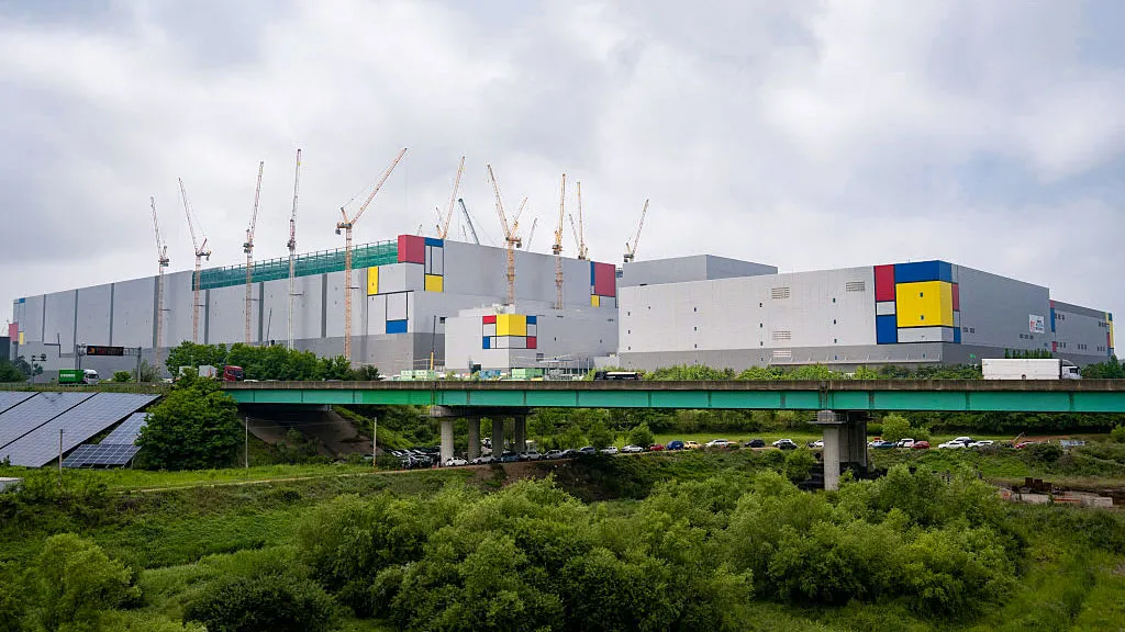
Publisher preview · OZZZER analysis pending editorial review.
PUBLISHER ARTICLE PREVIEW
From the original article
At the world’s biggest chipmaking complex, Samsung is building the fabs it needs for the AI memory boom.
Generative AI models run on powerful chips known as GPUs, which depend on stacks of specialized memory chips packaged with the processor. To meet growing demand for memory, Samsung is building a massive new semiconductor manufacturing complex in Pyeongtaek, South Korea. Three fabs already operate around the clock, and a fourth is coming online. Construction of a fifth was halted during a drop in demand for memory chips in 2024 but restarted when the AI boom sent demand soaring.
It’s just before noon on a Monday, and construction workers are pouring out of Samsung’s fabs in Pyeongtaek, a farming city south of Seoul where rice paddies abut a sprawling chipmaking complex. Thousands of workers, dressed head to toe in black with sky-blue vests, take off helmets bearing their names and fab numbers.
They walk to lunch, sweaty and flushed, in chunky sneakers capped with yellow rubber toe guards. Some hop on scooters or motorcycles to get around the campus, which covers an area about the size of New York City’s Central Park.
Source
MIT Technology Review · 20 Oct 2026 · 11:00 CEST
Open the original at MIT Technology Review ↗